

A few weeks ago, we showed the new IBM z17 Mainframe, which brings AI with Telum II and Spyre. I attended the launch, but the next day, I was able to tour IBM’s Fishkill facility, where they do engineering, including failure analysis. As part of that, we got some unique looks at hardware that few get to see.
There is a lot more in the video here:
We had to travel for this one, and we got special access. We need to say this is sponsored by IBM on anything we do related to that even if this was not a piece IBM asked us to do. It was, however, too cool for us to only have on video.
The New IBM z17 Telum II Processor
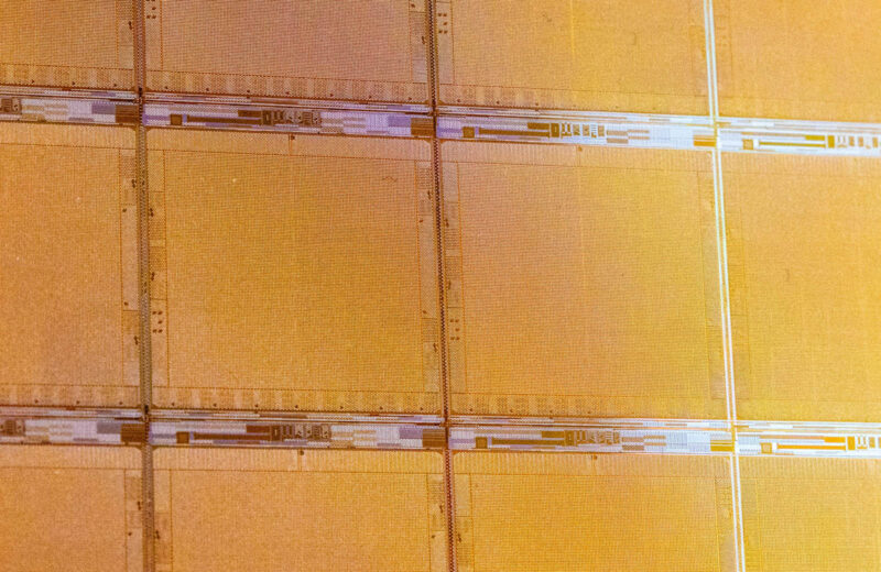
Something fun that we got to see during our visit to Fishkill is the IBM z17’s Telum II processor cut open for materials analysis. At the same time, IBM had a ton on display down to the wafers of Telum II processors.
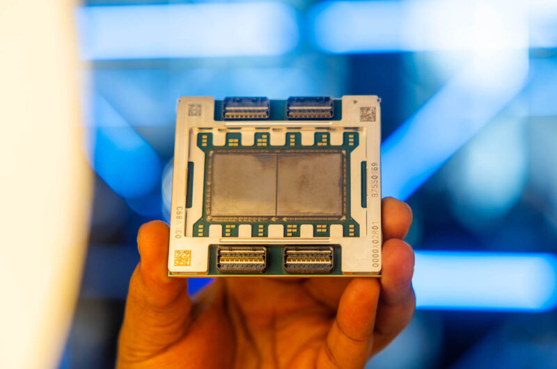
In our previous piece, we showed the dual chip modules or DCMs.
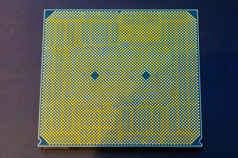
We also managed to grab a shot of the bottom pads.
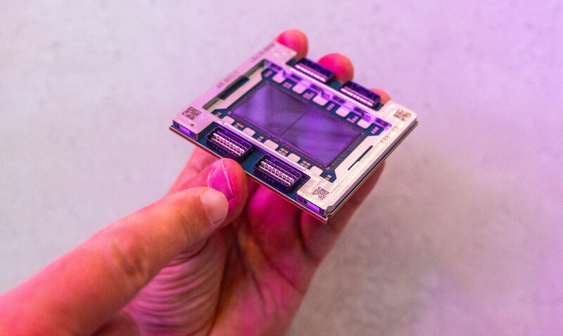
The socket itself is neat. Instead of the I/O being completely through those bottom pads, there are also SMP cable connectors that aid in processor to processor communication.
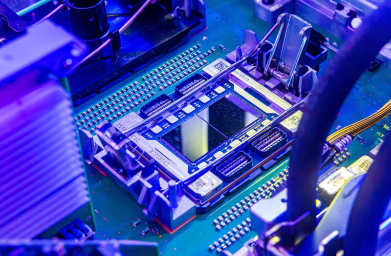
Here is another look at those.
Of course, this is just what we saw last time. I challenge IBM to show some behind-the-scenes of how these are made, and IBM let me into its Fishkill facility where we got down to the individual atom level. Let us get to that next.