Hot Chips 25 was held August 24-26 on the Stanford University campus again this year, with many exciting and interesting presentations. I’ve noticed an overall trend with more focus being placed on overall systems rather than the socket. As the conference name suggests, there’s a history of showcasing chips, but with the increased emphasis on AI and related large-scale computing, efficiency of the total system is also of primary importance.
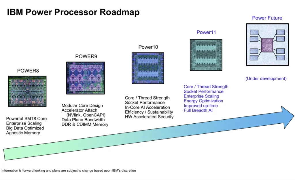
William Starke from IBM presented, “IBM’s Power11 Processor”. IBM announced Power11 on July 8, 2025, so this was more than a chip presentation, as systems are already being shipped. Their Power Processor roadmap is shown below. While IBM builds 2-4 socket systems, they also go up to 16 sockets. Although the IBM Power chips don’t typically have as many cores per socket as others, their emphasis is on higher per core performance.

Fig. 1: IBM Power Processor roadmap.
IBM sells to customers from small businesses to the world’s largest enterprises, so robust scaling is important to enable flexible deployments for on-prem, hybrid and public cloud scenarios. With modern workloads incorporating more AI, Starke said that he believes that system design and performance are going to be more important going forward and that a system-focused, instead of socket-focused approach is needed.
With 99.9999% of uptime, roughly equivalent to ~31.5 seconds of downtime per year, Power11 is designed to be the most resilient server in the history of the IBM Power platform. The article “Reducing Voltage Guard Band,” published this past March, looked at an IBM power management approach for exceptional reliability.
IBM claims customers for larger systems aren’t looking so much for more capacity but want faster thread performance, so IBM decided to go with Samsung’s Enhanced 7nm process rather than going to 5nm. IBM also worked with Samsung for their packaging of a 2.5D ISC Architecture.
Going from Power10 to Power11 (2-socket systems), the Power11 has 50% more cores at a higher clock speed. For the largest system, that translates into a boost in clock speed from 4.0 GHz to 4.3 GHz (with more cores).

Fig. 2: IBM Power10 to Power11 performance comparison.
Typically, industry implementations use direct attach memory, which isn’t very “beachfront” efficient and burns up quite a bit of the I/O space to communicate with say 8 DDR ports. Instead, IBM uses a hierarchical buffered memory architecture and goes through 16 intermediate buffers that connect to 32 DDR ports (2 DDR ports per buffer) per processor socket. This gives the IBM system effectively a 4x Bandwidth and 4x Capacity (per processor) advantage.
The communication between the processor and the buffers uses high-speed SerDes links running at 38.4 Gb that have very good resilience characteristics with excellent bandwidth and signal integrity.
Figure 3 below shows the specialized OMI DIMM form factor with the buffer chip sitting underneath the copper heatsink.

Fig. 3: IBM Power Processor OMI D-DIMM.
Since the buffer is attached to the D-DIMM, upgrading to newer versions of DDR is straightforward, as the communication from the processor to the memory is through the SerDes links.
Figure 4 below shows the newer Odyssey DDR5 2-port D-DIMM with a 50% increase in bandwidth on the DDR ports going from 25.6 GB/s to 38.4 GB/s and a 2x increase in ports going to 2-ports from 1-port in the older Explorer DDR4 D-DIMM. This gives the Power11 processor a 3x increase in DRAM bandwidth per socket and up to 8 TB of total DRAM capacity.

Fig. 4: IBM Power Processor roadmap.
The inclusion of in-core matrix math accelerators (MMA) in Power10 was a fortunate early feature that has paid dividends in terms of performance for accelerated AI large models and tuning. In addition, Power11 systems will also be able to utilize IBM’s external Spyre accelerators. IBM’s Chris Berry presented IBM Telum II Processor and IBM Spyre Accelerator Chip for AI at last year’s Hot Chips 2024. The IBM Spyre Accelerator is expected to be available in Q4 2025. So, in all, there are really 3 “Hot Chips” in the new system: the Power11, the Odyssey memory buffer, and the Spyre accelerator.
Figure 5 below provides some insight into the direction of the next-generation Power processor, referred to as “Power Future.” It will move to a chiplet-based architecture with an I/O hub in the center.

Fig. 5: IBM Power Processor roadmap – beyond Power11.
Using memory chips with SerDes clearly decreases beachfront and increases bandwidth. As features get smaller, the difference between on and off chip connectivity lines is 10x+. Chiplets also leverage packaging (2.5D interposer) technology.
The systems are buffered memory optimized and IBM has been working on this for decades. The SerDes run synchronously with the DDR on the buffer so that they can have extremely long predictable pipelines with several bypasses. The whole Power11 OMI memory is implemented in such a way that there’s only an extra 6-8ns of latency for going to memory. Starke stated that if you’re starting out with about 90-100ns of latency, the additional 6-8ns of latency isn’t really that noticeable and HBM doesn’t offer a high enough capacity now to fit their profile. For their target applications, capacity is really important, and IBM’s architecture enables this capacity in a very efficient manner.

